14.4. Environmental constraints
Both DRC and optimization
constraints follow environmental constraints. Setting up of operating
conditions and wire load model falls under environmental constraints.


Transition Delay
Transition delay or slew is defined as the time taken by signal to rise from 10 %( 20%) to the 90 %( 80%) of its maximum value. This is known as “rise time”.

Similarly “fall time” can be defined as the time taken by a signal to fall from 90 %( 80%) to the 10 %( 20%) of its maximum value.
Transition is the time it takes for the pin to change state.
Setting Transition Time Constraints
The above theoretical definitions are to be applied on practical designs. Now, the transition time of a net becomes the time required for its driving pin to change logic values (from 10 %( 20%) to the 90 %( 80%) of its maximum value). This transition time used foe delay calculations are based on the timing library (.lib files).
Transition related constraints can be provided in Design Compiler (logic synthesis tool from Synopsys) by using below commands:
1. max_transition : This attribute is applied to each output of a cell. During optimization, Design Compiler tries to make the transition time of each net less than the value of the max_transition attribute.
2. set_max_transition: This command is used to change the maximum transition time restriction specified in a technology library.
“This command sets a maximum transition time for the nets attached to the identified ports or to all the nets in a design by setting the max_transition attribute on the named objects.
For example, to set a maximum transition time of 3.2 on all nets in the design adder, enter the following command:
set_max_transition 3.2 [get_designs adder]
To undo a set_max_transition command, use the remove_attribute command. For example, enter the following command:
remove_attribute [get_designs adder] max_transition”
(Directly quoted from Design Complier user manual)
Setting Capacitance Constraints
The transition time constraints specified above do not provide a direct way to control the actual capacitance of nets. To control capacitance directly, below command has to be used:
set_max_capacitance: This command sets the maximum capacitance constraint on input ports or designs.
In addition to set_max_transition, set_max_capacitance can also be used as this command works independent.
This command applies maximum capacitance limit to output pin or port of the design.
This command can also be used to apply capacitance limit on any net.
Eg:
set_max_capacitance 4 [get_designs decoder]
To remove the set_max_capacitance command, use the remove_attribute command.
remove_attribute [get_designs decoder] max_capacitance
Propagation Delay
Hence if it is cell, you can call it as “Gate or Cell Delay” or if it is net you can call it as “Net Delay”
Propagation delay of a gate or cell is the time it takes for a signal at the input pin to affect the output signal at output pin.
For any gate propagation delay is measured between 50% of input transition to the corresponding 50% of output transition.
There are 4 possibilities:
Propagation delay between 50 % of Input rising to 50 % of output rising.
Propagation delay between 50 % of Input rising to 50 % of output falling.
Propagation delay between 50 % of Input falling to 50 % of output rising.
Propagation delay between 50 % of Input falling to 50 % of output falling.
Each of these delays has different values. Maximum and minimum values of these set are very important. Maximum and minimum propagation delay values are considered for timing analysis.
For net propagation delay is the delay between the time a signal is first applied to the net and the time it reaches other devices connected to that net.
Propagation delay is taken as the average of rise time and fall time i.e. Tpd= (Tphl+Tplh)/2.
Propagation delay depends on the input transition time (slew rate) and the output load. Hence two dimensional look up tables are used to calculate these delays. How to calculate propagation delay of net and gate? Please refer below articles to find the detailed explanation.
Contamination Delay:
Best case delay from valid input to valid output. i.e. minimum propagation delay.

There are several factors which affect net parasitic:
Net Length
Net cross-sectional area
Resistively of material used for metal layers (Aluminum vs. copper)
Number of vias traversed by the net
Proximity to other nets (crosstalk)
Interconnect introduces capacitive, resistive and inductive parasites. All three have multiple effects on the circuit behavior.
Interconnect parasites cause an increase in propagation delay (i.e. it slows down working speed)
Interconnect parasites increase energy dissipation and affect the power distribution.
Interconnect parasites introduce extra noise sources, which affect reliability of the circuit. (Signal Integrity effects)
Dominant parameters determine the circuit behavior at a given circuit node. Non-dominant parameters can be neglected for interconnect analysis.
Capacitance
Capacitance can be modeled by the parallel plate capacitor model.
C = (ε / t).WL
Where
ε --> permittivity of dielectric material (SiO2)
t --> thickness of dielectric material (SiO2)
W --> width of wire
L --> length of wire
ε --> εr εo where εr --> relative permittivity of SiO2
εo --> 8.854 x 10⁻¹² F/m; permittivity of free space
As technology node shrinks (scaling), to minimize resistance of the wires, it is desirable to keep the cross section of the wire (WxH) as large as possible. But this increases area. Small values of W lead to denser wiring and less area overhead. In advanced process W/H ratio has reduced below unity. Under such circumstances parallel plate capacitance model becomes inaccurate. The capacitance between the sidewall of the wires and substrate called fringing capacitance can no longer be ignored and contributes to the overall capacitance.

Inter-wire capacitance become dominant factor in multilayer interconnect structures. These floating capacitors (not connected to substrate or ground) form a source of noise (cross talk). This effect is more pronounced for wires in the higher interconnect layer, as these are farther away from the substrate.
Generally higher metal layers (i.e. interconnects) have higher thickness (i.e. height) and higher dielectric layers have higher permittivity. Hence these wires display the highest inter-wire capacitance. Hence use it for global signals that are not sensitive to interference. (eg. Supply rails). Or it is advisable to separate wires by an amount that is larger than minimum spacing.
~~~~~~~~~~~~~~~~~~~~~~~~~~~~~~~~~~~~~~~~~~~~~~~~~~~~~~~~~~~~~~~~~~~~~~~~~~~~
Resistance
Resistance R= (ρ.L)/ (H.W) = (ρ. L)/ Area
L --> length
W --> width
ρ --> resistivity (ohm-m)
Since H (height, thickness) is constant for a given technology we can write: R = Rs.(L/W) where Rs=ρ/H ohm/sqare is called “sheet resistance”.
At very high frequencies “skin effect” comes into play such that the resistance becomes frequency dependent. High frequency currents tend to flow primarily on the surface of a conductor, with the current density falling off exponentially with depth into the conductor.
Skin effect is only an issue for wider wires. Since clocks tends to carry the highest frequency signals on a chip and also fairly wide to limit resistance, the skin effect likely to have its first impact on these lines.
~~~~~~~~~~~~~~~~~~~~~~~~~~~~~~~~~~~~~~~~~~~~~~~~~~~~~~~~~~~~~~~~~~~~~~~~~~~~
Inductance
With the adoption of low resistance interconnect materials and the increase of switching frequencies to GHz range, inductance starts to an important role. Consequences of on chip inductance include ringing and overshoot effect, reflection of signals due to impedance mismatch, inductive coupling between lines, and switching noise due to (Ldi/dt) voltage drops.
~~~~~~~~~~~~~~~~~~~~~~~~~~~~~~~~~~~~~~~~~~~~~~~~~~~~~~~~~~~~~~~~~~~~~~~~~~~~
Lumped Capacitor Model
As long as the resistive component of the wire is small, and switching frequencies are in the low to medium range, it is meaningful to consider only the capacitive component of the wire, and to lump the distributed capacitance into a single capacitance.

The only impact on performance is introduced by the loading effect of the capacitor on the driving gate.
~~~~~~~~~~~~~~~~~~~~~~~~~~~~~~~~~~~~~~~~~~~~~~~~~~~~~~~~~~~~~~~~~~~~~~~~~~~
Lumped RC Model
If wire length is more than a few millimeters, the lumped capacitance model is inadequate and a resistive capacitive model has to be adopted.
In lumped RC model the total resistance of each wire segment is lumped into one single R, combines the global capacitive into single capacitor C.
Analysis of network with larger number of R and C becomes complex as network contains many time constants (zeroes and poles). Elmore delay model overcome such problem.
~~~~~~~~~~~~~~~~~~~~~~~~~~~~~~~~~~~~~~~~~~~~~~~~~~~~~~~~~~~~~~~~~~~~~~~~~~~~
Elmore Delay Model

Properties of the network:
“Path resistance” is the resistance from source node to any other node.
“Shared path resistance” is the resistance shared among the paths from the source node to any other two nodes.
Hence,
Delay at node 1: Tow d1 = R1C1
Delay at node 2: Tow d2= (R1+R2)C2
Delay at node 3: Tow d3 = (R1+R2+R3)C3
In general:
τdi=R1C1+(R1+R2)C2+……..+(R1+R2+R3+…..+Ri)Ci
If
R1=R2=R3=….=R
C1=C2=C3=…..C then
τdi=RC+2RC+……..+nRC
Thus Elmore delay is equivalent to the first order time constant of the network.
Assuming an interconnect wire of length L is partitioned into N identical segments. Each segment has length L/N.
Then,
τd=L/N.R.L/N.C+ 2 (L/n.r+L/N.C)+……
=(L/N)2(RC+2RC+…….+NRC)
=(L/N)2. N(N+1)
or τd=RC.L2/2
=> The delay of a wire is a quadratic function of its length
=> doubling the length of the wire quadruples its delay
Advantages
Disadvantages
Extraction data from already routed designs are used to build a lookup table known as the wire load model (WLM). WLM is based on the statistical estimates of R and C based on “Net Fan-out”.
wire_load (“5KGATES”) {
resistance : 0.000271 -------------> R per unit length
capacitance : 0.00017 -------------> C per unit length
slope : 29.4005 ---------------------> Used for linear extrapolation
fanout_length (1, 18.38) ----------> (fanout = 1, length = 18.38)
fanout_length (2, 47.78)
fanout_length (3, 77.18)
fanout_length (4, 106.58)
fanout_length (5, 135.98)
}
Eg:
Fanout = 7
Net length = 135.98 + 2 x 29.4005 (slope) = 194.78 ----------> length of net with fanout of 7
Resistance = 194.78 x 0.000271 = 0.05279 units
Capacitance = 194.78 x 0.00017 = 0.03311 units
Wire load modeling allows us to estimate the effect of wire length and fanout on the resistance, capacitance, and area of nets. Synthesizer uses these physical values to calculate wire delays and circuit speeds. Semiconductor vendors develop wire load models, based on statistical information specific to the vendors’ process. The models include coefficients for area, capacitance, and resistance per unit length, and a fanout-to-length table for estimating net lengths (the number of fanouts determines a nominal length).
Selection of wire load models in the initial stage (before physical design) depends on the fallowing factors:
1. User specification
2. Automatic selection based on design area
3. Default specification in the technology library
Once the final routing step is over in the physical design stage, wire load models are generated based on the actual routing in the design and synthesis is redone using those wire load models.
In hierarchical designs, we have to determine which wire load model to use for nets that cross hierarchical boundaries. There are three modes for determining which wire load model to use for nets that cross hierarchical boundaries:
Top:
Applying same wire load models to all nets as if the design has no hierarchy and uses the wire load model specified for the top level of the design hierarchy for all nets in a design and its sub designs.

The wire load model of the smallest design that fully encloses the net is applied. If the design enclosing the net has no wire load model, then traverses the design hierarchy upward until we finds a wire load model. Enclosed mode is more accurate than top mode when cells in the same design are placed in a contiguous region during layout.
Use enclosed mode if the design has similar logical and physical hierarchies.
Segmented:
Wire load model for each segment of a net is determined by the design encompassing the segment. Nets crossing hierarchical boundaries are divided into segments. For each net segment, the wire load model of the design containing the segment is used. If the design contains a segment that has no wire load model, then traverse the design hierarchy upward until it finds a wire load model.Interconnect Delay vs. Deep Sub Micron Issues
Performances of deep sub micron ICs are limited by increasing interconnect loading affect. Long global clock networks account for the larger part of the power consumption in chips. Traditional CAD design methodologies are largely affected by the interconnect scaling. Capacitance and resistance of interconnects have increased due to the smaller wire cross sections, smaller wire pitch and longer length. This has resulted in increased RC delay. As technology is advancing scaling of interconnect is also increasing. In such scenario increased RC delay is becoming major bottleneck in improving performance of advanced ICs.
Limits of Cu/low-k interconnects
At submicron level of 250 nm copper with low-k dielectric was introduced to decrease affects of increasing interconnect delay. But below 130 nm technology node interconnect delays are increasing further despite of introducing low-k dielectric. As the scaling increases new physical and technological effects like resistivity and barrier thickness start dominating and interconnect delay increases. Introduction of repeaters to shorten the interconnect length increases total area. The vias connecting repeaters to global layers can cause blockage in lower metal layers. Thus as the technology improves material limitations will dominate factor in the interconnect delay. Increasing metal layer width will cause increase in metallization layer. This can’t be a solution for the problem as it increases complexity, reliability and cost.
Cu low-k dielectric films are deposited by a special process known as Damascene process. Adhesion property of Cu with dielectric materials is very poor. Under electric bias they easily drift and cause short between metal layers. To avoid this problem a barrier layer is deposited between dielectric and Cu trench. Even though it decreases effective cross section of interconnects compared to drawn dimensions, it improves reliability. The barrier thickness becomes significant in deep submicron level and effective resistance of the interconnect rises further. In addition to this increasing electron scattering and self heating caused by the electron flow in interconnects due to comparable increase in internal chip temperature also contribute to increase interconnect resistance.
~~~~~~~~~~~~~~~~~~~~~~~~~~~~~~~~~~~~~~~~~~~~~~~~~~~~~~~~~~~~~~~~~~~~~~~~~~~~We encounter several types of delays in ASIC design. They are as follows:
Wire delays or extrinsic delays are calculated using output drive strength, input capacitance and wire load models. Other delays are intrinsic properties of each and every gate.
Delays are interdependent on different electrical properties. [Nekoogar]:
Gate Delay
Transistors within a gate take a finite time to switch. This means that a change on the input of a gate takes a finite time to cause a change on the output. [Magma]
Gate delay =function of (input transition (slew) time, Cnet+Cpin).
or
Gate delay =function of (input transition (slew) time, Cload).
where Cload=Cnet+Cpin
Cnet-->Net capacitance
Cpin-->pin capacitance of the driven cell
Cell delay is also same as Gate delay.

How gate delay is calculated?
Cell or gate delay is calculated using Non-Linear Delay Models (NLDM). NLDM is highly accurate as it is derived from SPICE characterizations. The delay is a function of the input transition time (i.e. slew) of the cell, the wire capacitance and the pin capacitance of the driven cells. A slow input transition time will slow the rate at which the cell’s transistors can change state logic 1 to logic 0 (or logic 0 to logic 1), as well as a large output load Cload (Cnet + Cpin), thereby increasing the delay of the logic gate.
There is another NLDM table in the library to calculate output transition. Output transition of a cell becomes the input transition of the next cell down the chain.
Table models are usually two-dimensional to allow lookups based on the input slew and the output load (Cload). A sample table is given below.
timing() {
related_pin : "CKN";
timing_type : falling_edge;
timing_sense : non_unate;
cell_rise(delay_template_7x7) {
index_1 ("0.012, 0.032, 0.074, 0.154, 0.318, 0.644, 1.3");
index_2 ("0.001278, 0.0046008, 0.0112464, 0.0245376, 0.05112, 0.10454, 0.212148");
values ( \
"0.225894, 0.249015, 0.285537, 0.352680, 0.484244, 0.748180, 1.279570", \
"0.231295, 0.254415, 0.290938, 0.358081, 0.489646, 0.753585, 1.284980", \
"0.243754, 0.266878, 0.303398, 0.370542, 0.502105, 0.766044, 1.297440", \
"0.267240, 0.290389, 0.326908, 0.394052, 0.525615, 0.789561, 1.320950", \
"0.307080, 0.330200, 0.366721, 0.433861, 0.565425, 0.829373, 1.360760", \
"0.380552, 0.403875, 0.440426, 0.507569, 0.639136, 0.903084, 1.434500", \
"0.497588, 0.521769, 0.558548, 0.625744, 0.757301, 1.021260, 1.552680");
}
rise_transition(delay_template_7x7) {
index_1 ("0.012, 0.032, 0.074, 0.154, 0.318, 0.644, 1.3");
index_2 ("0.001278, 0.0046008, 0.0112464, 0.0245376, 0.05112, 0.10454, 0.212148");
values ( \
"0.040574, 0.068619, 0.125391, 0.246672, 0.497688, 1.005982, 2.030120", \
"0.040570, 0.068618, 0.125390, 0.246672, 0.497688, 1.005940, 2.030240", \
"0.040565, 0.068616, 0.125389, 0.246650, 0.497770, 1.006180, 2.030120", \
"0.040532, 0.068612, 0.125387, 0.246670, 0.497710, 1.006164, 2.030100", \
"0.040578, 0.068621, 0.125392, 0.246636, 0.497688, 1.006182, 2.030040", \
"0.041763, 0.069211, 0.125662, 0.246758, 0.497726, 1.005930, 2.030000", \
"0.045813, 0.071321, 0.126671, 0.247154, 0.497846, 1.005962, 2.030180");
}
index_1 --> input transition values
index_2--> output load capacitance values
values--> delay values
Situation 1:
Input transition and output load values match with table index values
If both input transition and output load values match with table index values then corresponding delay value is directly picked up from the delay “values” table as highlighted by yellow shaded data.
Situation 2:
Output load values doesn't match with table index values
When the actual load capacitance values does not fall directly on or at one of the load-axis index points, the delay is determined by interpolation from the closest points. Note that to carry out interpolation input transition point should match with the any one of the table index values.
Determine the equation for the line segment connecting the two nearest points in the table.
To do this first we need to find the slope value.
Slope m = (y2-y1)/(x2-x1) where (y2-y1) is delay segment (generally in ns) on y axis and (x2-x1) is load segment (generally in pf) on x-axis.
Solve for the delay at the load point of interest.
The linear equation is:
y = mx+c
where
y-->delay (ns)
m-->slope
x-->load capacitance (pf)
i.e. delay=slope*load point of interest (constant value is zero)
Load point of interest means load capacitance value for which delay has to be calculated.
Situation 3:
Both input transition and output load values doesn't match with table index values
If both input transition and load capacitance values do not match exactly with the look up table index values then bilinear interpolation is used.
Multiple linear interpolations (~3) are performed on multiple closest table data points (~4) as shown in highlighted violet color in the look up table.
Situation 4:
Output load values doesn't match with table index values and is outside the table boundary
When the load point is outside of the boundary of the index, the delay is extrapolated to the closest known points.
Lookup value too far out of range of the given table value could lead to inaccuracy. [Cadence]
Intrinsic delay
[Nekoogar] Farzad Nekoogar, “Timing Verification of Application Specific Integrated Circuits”, Prentice Hall
[Magma] Magma Blast Fusion User Guides
[Cadence] Cadence SOC Encounter User Guides
Dynamic timing analysis has to be accomplished and functionality of the design must be cleared before the design is subjected to Static Timing Analysis (STA). Dynamic Timing Analysis (DTA) and Static Timing Analysis (STA) are not alternatives to each other. Quality of the Dynamic Timing Analysis (DTA) increases with the increase of input test vectors. Increased test vectors increase simulation time. Dynamic timing analysis can be used for synchronous as well as asynchronous designs. Static Timing Analysis (STA) can’t run on asynchronous deigns and hence Dynamic Timing Analysis (DTA) is the best way to analyze asynchronous designs. Dynamic Timing Analysis (DTA) is also best suitable for designs having clocks crossing multiple domains.
Example of Dynamic Timing Analysis(DTA) tool is Modelsim (from mentor Graphics), VCS (from Synopsys). DTA is also carried out on post layout netlist to verify that functionality of the design has not changed. Test vectors remain same for both.
SPICE Simulation
What is Static Timing Analysis (STA)?
In Static Timing Analysis (STA) static delays such as gate delay and net delays are considered in each path and these delays are compared against their required maximum and minimum values. Circuit to be analyzed is broken into different timing paths constituting of gates, flip flops and their interconnections. Each timing path has to process the data within a clock period which is determined by the maximum frequency of operation. Cell delays are available in the corresponding technology libraries. Cell delay values are tabulated based on input transition and fanout load which are characterized by SPICE simulation. Net delays are calculated based on the Wire Load Models(WLM) or extracted resistance R and capacitance C. Wire Load Models(WLM) are available in the Technology File. These values are Table Look Up(TLU) values calculated based on the net fanout length.
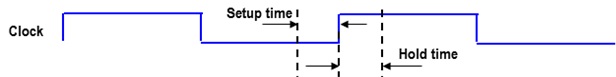
The static timing analyzer will report the following delays (or it can do following analysis):
Register to Register delays
Setup times of all external synchronous inputs
Clock to Output delays
Pin to Pin combinational delays
Different Analysis Modes-Best, Worst, Typical, On Chip Variation (OCV)
Data to Data Checks
Case Analysis
Multiple Clocks per Register
Minimum Pulse Width Checks
Derived Clocks
Clock Gating Checks
Netlist Editing
Report_clock_timing
Clock Reconvergence Pessimism
Worst-Arrival Slew Propagation
Path-Based Analysis
Debugging Delay Calculation
and many more......!!
The wide spread use of STA can be attributed to several factors [David]:
The basic STA algorithm is linear in runtime with circuit size, allowing analysis of designs in excess of 10 million instances.
The basic STA analysis is conservative in the sense that it will over-estimate the delay of long paths in the circuit and under-estimate the delay of short paths in the circuit. This makes the analysis ”safe”, guaranteeing that the design will function at least as fast as predicted and will not suffer from hold-time violations.
The STA algorithms have become fairly mature, addressing critical timing issues such as interconnect analysis, accurate delay modeling, false or multi-cycle paths, etc.
Delay characterization for cell libraries is clearly defined, forms an effective interface between the foundry and the design team, and is readily available. In addition to this, the Static Timing Analysis (STA) does not require input vectors and has a runtime that is linear with the size of the circuit [Agarwal].
Advantages of STA:
Disadvantages of STA:
References
[David] David Blaauw, Kaviraj Chopra, Ashish Srivastava and Lou Scheffer, “Statistical Timing Analysis: From basic principles to state-of-the-art.”, Transactions on Computer-Aided Design of Integrated Circuits and Systems (T-CAD), IEEE.
[Agarwal] Agarwal, A. Blaauw, D. Zolotov, V. Sundareswaran, S. Min Zhao Gala, K. and Panda, R., “Statistically Delay computation considering spatial correlations,” Proceedings of the ASP-DAC 2003, pp.271-276, Jan 2003.
Below interview questions are contributed by ASIC_diehard (Thanks a lot !). Below questions are asked for senior position in Physical Design domain. The questions are also related to Static Timing Analysis and Synthesis. Answers to some questions are given as link. Remaining questions will be answered in coming blogs.
Common introductory questions every interviewer asks are:
Intel
The resistivity of top metal layers are less and hence less IR drop is seen in power distribution network. If power stripes are routed in lower metal layers this will use good amount of lower routing resources and therefore it can create routing congestion.
Answer:
This approach allows routability of the design and better usage of routing resources.
Answer:
Improve the input transition to the cell under consideration by up sizing the driver.
Reduce the load seen by the cell under consideration, either by placement refinement or buffering.
If allowed increase the drive strength or replace with LVT (low threshold voltage) cell.
Answer:
Logic optimization: buffer sizing, cell sizing, level adjustment, dummy buffering etc.
Less number of logics between Flip Flops speedup the design.
Optimize drive strength of the cell , so it is capable of driving more load and hence reducing the cell delay.
Better selection of design ware component (select timing optimized design ware components).
Use LVT (Low threshold voltage) and SVT (standard threshold voltage) cells if allowed.
Answer:
Set don’t use attribute on those library cells.
Answer:
Routing and placement congestion all depend upon the connectivity in the netlist , a better floor plan can reduce the congestion.
Noise can be reduced by optimizing the overlap of nets in the design.
Answer:
No. You should not increase clock buffers in the clock network. Increase in clock buffers cause more area , more power. When everything is fine why you want to touch clock tree??
Answer:
Better skew targets and insertion delay values provided while building the clocks.
Choose appropriate tree structure – either based on clock buffers or clock inverters or mix of clock buffers or clock inverters.
For multi clock domain, group the clocks while building the clock tree so that skew is balanced across the clocks. (Inter clock skew analysis).
STmicroelectronics
Texas Instruments (TI)
Qualcomm
Answer:
set_clock_uncertainty –from
Difference in clock uncertainty values; Clocks are propagated in post CTS.
In post CTS clock latency constraint is modified to model clock jitter.
Answer:
Make the clock gating cells as through pins.
Hughes Networks
Avago Technologies (former HP group)
Hynix Semiconductor
About Contributor
ASIC_diehard has more than 5 years of experience in physical design, timing, netlist to GDS flows of Integrated Circuit development. ASIC_diehard's fields of interest are backend design, place and route, timing closure, process technologies.
Readers are encouraged to discuss answers to these questions. Just click on the 'post a comment' option below and put your comments there. Alternatively you can send your answers/discussions to my mail id: shavakmm@gmail.com