1) Power consumed by combinatorial logic whose values are changing on each clock edge
2) Power consumed by flip-flops and
3) The power consumed by the clock buffer tree in the design.
It is good design idea to turn off the clock when it is not needed. Automatic clock gating is supported by modern EDA tools. They identify the circuits where clock gating can be inserted.
RTL clock gating works by identifying groups of flip-flops which share a common enable control signal. Traditional methodologies use this enable term to control the select on a multiplexer connected to the D port of the flip-flop or to control the clock enable pin on a flip-flop with clock enable capabilities. RTL clock gating uses this enable signal to control a clock gating circuit which is connected to the clock ports of all of the flip-flops with the common enable term. Therefore, if a bank of flip-flops which share a common enable term have RTL clock gating implemented, the flip-flops will consume zero dynamic power as long as this enable signal is false.
There are two types of clock gating styles available. They are:
1) Latch-based clock gating
2) Latch-free clock gating.
Latch free clock gating
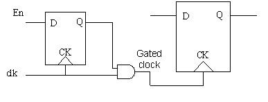
The latch-free clock gating style uses a simple AND or OR gate (depending on the edge on which flip-flops are triggered). Here if enable signal goes inactive in between the clock pulse or if it multiple times then gated clock output either can terminate prematurely or generate multiple clock pulses. This restriction makes the latch-free clock gating style inappropriate for our single-clock flip-flop based design.
Latch free clock gating
Latch based clock gating
The latch-based clock gating style adds a level-sensitive latch to the design to hold the enable signal from the active edge of the clock until the inactive edge of the clock. Since the latch captures the state of the enable signal and holds it until the complete clock pulse has been generated, the enable signal need only be stable around the rising edge of the clock, just as in the traditional ungated design style.
Latch based clock gating
Specific clock gating cells are required in library to be utilized by the synthesis tools. Availability of clock gating cells and automatic insertion by the EDA tools makes it simpler method of low power technique. Advantage of this method is that clock gating does not require modifications to RTL description.
References
[1] Frank Emnett and Mark Biegel, “Power Reduction Through RTL Clock Gating”, SNUG, San Jose, 2000
[2] PrimeTime User Guide


Mention that one has to use negative-level sensitive latch for a pos-edge flop design. So I would prefer you indicating a bubble infront of latch
ReplyDeleteyou are right
Deleteyou are right......... thanks for the observation !
ReplyDeleteSo how does the timing between the neg-edge latch and the pos-edge flop look like ? I am not sure if it's a half-cycle path or a full cycle path.
ReplyDeleteCan you please clarify if possible.
Latch to flop is just a clock path. So you don't need to check timing between them. Instead you have two timing path checks which involves latch. First one is from Enable start point to latch and second is with pos-edge flop normal check and here we need to treat latch as transparent in clock path
DeleteOr use a pos-edge flip-flip instead of a latch. (For gating pos-edge clocked flip-flops.)
ReplyDeleteThen you don't have to use latches, which can make DFT harder in some cases.
If someone is not using Library available hard cell for clock gating , and writing it's own code for the same , how will the user make sure for timing analysis for this ?? How to define constraints for the same. ???
ReplyDeleteCan timing diagrams for latch based gating be included too?
ReplyDeleteThe bubble on the latch has also not been included?
Hi Murali,
ReplyDeleteNice explanation.
Why your latch & flip flop symbols are same ?
Can you please update the latch symbol.
I believe it is not good practice to use the triangle symbol on the input to a level-sensitive latch. The triangle denotes edge-triggered, which is correct for the main, master-slave flip flops, but the glitch-removing latch is a transparent one.
ReplyDeleteUsing a flip-flop is better than a latch, b'coz if the latch is negative level one and EN signal changes during the negative edge of clock, then it also produces same possible glitches as produced in latch-free gating.... So I think use of flip-flop is better than latch.. Did I miss anything here??
ReplyDeleteWhether to use a negative latch or a positive level latch depends upon the FFs that are going to be triggered. So if all the FFs are +ve edge trigger, than a -ve latch is sufficient because it will pass the enable the signal at negative level(which is inactive period of FFs) so it won't create any glitch.
DeleteCorrect me if I'm wrong.
how do you reduce power?
ReplyDeleteGood article on types of clock gating.
ReplyDeleteWhat is the reason if clock gating cell has no clock
ReplyDeleteI would like to show thanks to you for amazing blog. You can also read our blog : promotional clocks
ReplyDelete