Showing posts with label Multi Vt. Show all posts

Issues with Multi Height Cell Placement in Multi Vt Flow

Creating the reference libraries

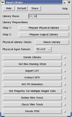
There are two reference libraries required. One is low Vt cell library and another is high Vt cell library. These libraries have two different height cells. Reference libraries are created as per the standard synopsys flow. Library creation flow is given in Figure 1. Read_lib command is used for this purpose. As TF and LEF files are available TF+LEF option is chosen for library creation. After the completion of the physical library preparation steps, logical libraries are prepared.


Figure 1 Library preparation command window


Different Unit Tile Creation

The unit tile height of lvt cells is 2.52 µ and hvt cells are 1.96 µ. Hence two separate unit tiles have to be created and should be added in the technology file. Hvt reference library is created with the unit tile name “unit” and lvt reference library is created with unit tile name “lvt_unit”. By default “unit” tile is defined in technology file and the other unit tile “lvt_unit” is also added to the technology file.


Figure 2. Tile height specifications in library preparation


Floor Planning

70% of the core utilization is provided. Aspect ratio is kept at 1. Rows are flipped, double backed and made channel less. No Top Design Format (TDF) file is selected as default placement of the IO pins are considered. Since we have multi height cells in the reference library separate placement rows have to be provided for two different unit tiles. The core area is divided into two separate unit tile section providing larger area for Hvt unit tile as shown in the Figure 3.


Figure 3. Different unit tile placement

First as per the default floor planning flow rows are constructed with unit tile. Later rows are deleted from the part of the core area and new rows are inserted with the tile “lvt_unit”. Improper allotment of area can give rise to congestion. Some iteration of trial and error experiments were conducted to find best suitable area for two different unit tiles. The “unit” tile covers 44.36% of core area while “lvt_unit” 65.53% of the core area. PR summary report of the design after the floor planning stage is provided below.


PR Summary:

Number of Module Cells: 70449

Number of Pins: 368936

Number of IO Pins: 298

Number of Nets: 70858

Average Pins Per Net (Signal): 3.20281

Chip Utilization:

Total Standard Cell Area: 559367.77

Core Size: width 949.76, height 947.80; area 900182.53

Chip Size: width 999.76, height 998.64; area 998400.33

Cell/Core Ratio: 62.1394%

Cell/Chip Ratio: 56.0264%

Number of Cell Rows: 392


Placement Issues with Different Tile Rows


Legal placement of the standard cells is automatically taken care by Astro tool as two separate placement area is defined for multi heighten cells. Corresponding tile utilization summary is provided below.


PR Summary:

[Tile Utilization]

============================================================

unit 257792 114353 44.36%

lvt_unit 1071872 702425 65.53%

============================================================

But this method of placement generates unacceptable congestion around the junction area of two separate unit tile sections. The congestion map is shown in Figure 4.


Figure 4. Congestion

There are two congestion maps. One is related to the floor planning with aspect ratio 1 and core utilization of 70%. This shows horizontal congestion over the limited value of one all over the core area meaning that design can’t be routed at all. Hence core area has to be increased by specifying height and width. The other congestion map is generated with the floor plan wherein core area is set to 950 µm. Here we can observe although congestion has reduced over the core area it is still a concern over the area wherein two different unit tiles merge as marked by the circle. But design can be routable and can be carried to next stages of place and route flow provided timing is met in subsequent implementation steps.


Tighter timing constraints and more interrelated connections of standard cells around the junction area of different unit tiles have lead to more congestion. It is observed that increasing the area isn't a solution to congestion. In addition to congestion, situation verses with the timing optimization effort by the tool. Timing target is not able to meet. Optimization process inserts several buffers around the junction area and some of them are placed illegally due to the lack of placement area.


Corresponding timing summary is provided below:


Timing/Optimization Information:

[TIMING]

Setup Hold Num Num

Type Slack Num Total Target Slack Num Trans MaxCap Time

========================================================

A.PRE -3.491 3293 -3353.9 0.100 10000.000 0 8461 426 00:02:26

A.IPO -0.487 928 -271.5 0.100 10000.000 0 1301 29 00:01:02

A.IPO -0.454 1383 -312.8 0.100 10000.000 0 1765 36 00:01:57

A.PPO -1.405 1607 -590.9 0.100 10000.000 0 2325 32 00:00:58

A.SETUP -1.405 1517 -466.4 0.100 -0.168 6550 2221 31 00:04:10

========================================================


Since the timing is not possible to meet design has to be abandoned from subsequent steps. Hence in a multi vt design flow cell library with multi heights are not preferred.


References

[1] Astro, User Guide, Version X-2005.09, September 2005


Multiple Threshold CMOS (MTCMOS) Circuits

James T. Kao et al. [2] showed MTCMOS logic is effective standby leakage control technique, but difficult to implement since sleep transistor sizing is highly dependent on discharge pattern within the circuit block. They showed dual Vt domino logic avoids the sizing difficulties and inherent performance associated with MTCMOS. High Vt cells are used where leakage has to be prevented whereas low Vt cells are employed where speed is of concern. Both cells are effectively used in MTCMOS technique.


MTCMOS technique [1]

In active mode of operation the high Vt transistors are turned off and the logic gates consisting of low Vt transistors can operate with low switching power dissipation and smaller propagation delay. In standby mode the high Vt transistors are turned off thereby cutting off the internal low Vt circuitry.


Variable Threshold CMOS (VTCMOS)

One of the efficient methods to reduce power consumption is to use low supply voltage and low threshold voltage without loosing speed performance. But increase in the lower threshold voltage devices leads to increased sub threshold leakage and hence more standby power consumption. Variable Threshold CMOS (VTCMOS) devices are one solution to this problem. In VTCMOS technique threshold voltage of the low threshold devices are varied by applying variable substrate bias voltage from a control circuitry.


VTCMOS technique is very effective technique to reduce the power consumption with some drawbacks with respect to manufacturing of these devices. VTCMOS requires either twin well or triple well technology to achieve different substrate bias voltage levels at different parts of the IC. The area overhead of the substrate bias control circuitry is negligible. [1]


References

[1] Sung Mo Kang and Yusuf Leblebici, “CMOS Digital Integrated Circuits-Analysis and Design”, Tata McGraw Hill, Third Edition, New Delhi, 2003

[2] James T. Kao and Anantha P. Chandrakasan, “Dual-Threshold Voltage Techniques for Low-Power Digital Circuits”, IEEE Journal Of Solid-state Circuits, Vol. 35, No. 7, pp.1009-1018, July 2000


Multi Threshold (MVT) Voltage Technique

Multiple threshold voltage techniques use both Low Vt and High Vt cells. Use lower threshold gates on critical path while higher threshold gates off the critical path. This methodology improves performance without an increase in power. Flip side of this technique is that Multi Vt cells increase fabrication complexity. It also lengthens the design time. Improper optimization of the design may utilize more Low Vt cells and hence could end up with increased power!

Ruchir Puri et al. [2] have discussed the design issues related with multiple supply voltages and multiple threshold voltages in the optimization of dynamic and static power. They noted several advantages of Multi Vt optimization. Multi Vt optimization is placement non disturbing transformation. Footprint and area of low Vt and high Vt cells are same as that of nominal Vt cells. This enables time critical paths to be swapped by low Vt cells easily.


Frank Sill et al. [3] have proposed a new method for assignment of devices with different Vth in a double Vth process. They developed mixed Vth gates. They showed leakage reduction of 25%. They created a library of LVT, mixed Vt, HVT and Multi Vt. They compared simulation results with a LVT version of each design. Leakage power dissipation decreased by average 65% with mixed Vth technique compared to the LVT implementation.


Meeta Srivatsav et al. [4] have explored various ways of reducing leakage power and recommended Multi Vt approach. They have carried out analysis using 130 nm and 90 nm technology. They synthesized design with different combination of target library. The combinations were Low Vt cells only, High Vt cells only, High Vt cells with incremental compile using Low Vt library, nominal (or regular) Vt cell and Multi Vt targeting Hvt and Lvt in one go. With only Low Vt highest leakage power of 469 µw was obtained. With only High Vt cells leakage power consumption was minimum but timing was not met (-1.13 of slack). With nominal Vt moderate leakage power value of 263 µw was obtained. Best results (54 µw with timing met) obtained for synthesis targeting Hvt library and incremental compile using Lvt library.


Different low leakage synthesis flows are carried out by Xiaodong Zhang [1] using Synopsys EDA tools are listed below:


  • Low-Vt --> Multi-Vt flow: This produces least cell count and least dynamic power. But produce highest leakage power. It takes very low runtime. Good for a design with very tight timing constraints


  • Multi-Vt one pass flow: It takes longest runtime and can be used in most of designs.


  • High-Vt --> Multi-Vt flow: Produce least leakage power consumption but has high cell count and dynamic power. This methodology is good for leakage power critical design.


  • High-Vt --> Multi-Vt with different timing constraints flow: This is a well balanced flow and produces second least leakage power. This has smaller cell count, area and dynamic power and shorter runtime. This design is also good for most of designs.


Optimization Strategies


The tradeoffs between the different Vt cells to achieve optimal performance are especially beneficial during synthesis technology gate mapping and placement optimization. The logic synthesis, or gate mapping phase of the optimization process is implemented by synthesis tool, and placement optimization is handled physical implementation tool.


Synthesis

During logic synthesis, the design is mapped to technology gates. At this point in the process optimal logic architectures are selected, mapped to technology cells, and optimized for specific design goals. Since a range of Vt libraries are now available and choices have to be made across architectures with different Vt cells, logic synthesis is the ideal place to start deploying a mix of different Vt cells into the design.


Single-Pass vs. Two-Pass Synthesis –with multiple threshold libraries


Multiple libraries are currently available with different performance, area and power utilization characteristics, and synthesis optimization can be achieved using either one or more libraries concurrently. In a single-pass flow, multiple libraries can be loaded into synthesis tool prior to synthesis optimization. In a two-pass flow, the design is initially optimized using one library, and then an incremental optimization is carried out using additional libraries.


About multi vt optimization in his paper Ruchir Puri[2] says: “The multi-threshold optimization algorithm implemented in physical synthesis is capable of optimizing several Vt levels at the same time. Initially, the design is optimized using the higher threshold voltage library only. Then, the Multi-Vt optimization computes the power-performance tradeoff curve up to the maximum allowable leakage power limit for the next lower threshold voltage library. Subsequently, the optimization starts from the most critical slack end of this power-performance curve and switches the most critical gate to next equivalent lower-Vt version. This will increase the leakage in the design beyond the maximum permissible leakage power. To compensate for this, the algorithm picks the least critical gate from the other end of the power-performance curve and substitutes it back with its higher-Vt version. If this does not bring the leakage power below the allowed limit, it traverses further from the curve (from least critical towards more critical) substituting gates with higher-Vt gates, until the leakage limit is satisfied. Then we jump back to the second most critical cell and switch it to the lower-Vt version. This iteration continues until we can no longer switch any gate with the lower vt version without violating the leakage power limit.”


But Amit Agarwal et al. [5] have warned about the yield loss possibilities due to dual Vt flows. They showed that in nano-scale regime, conventional dual Vt design suffers from yield loss due to process variation and vastly overestimates leakage savings since it does not consider junction BTBT (Band To Band Tunneling) leakage into account. Their analysis showed the importance of considering device based analysis while designing low power schemes like dual Vt. Their research also showed that in scaled technology, statistical information of both leakage and delay helps in minimizing total leakage while ensuring yield with respect to target delay in dual Vt designs. However, nonscalability of the present way of realizing high Vt, requires the use of different process options such as metal gate work function engineering in future technologies.


References

[1] Xiaodong Zhang, “High Performance Low Leakage Design Using Power Compiler and Multi-Vt Libraries”, Synopsys, SNUG, Europe, 2003, www.synopsys.com, 10/9/2007

[2] Ruchir Puri, “Minimizing Power Under Performance Constraint”, International Conference on Integrated Circuit Design and technology, IEEE, pp.159-163, May 17-20 2004

[3] Frank Sill, Frank Grassert and Dirk Timmermann, “Reducing Leakage with Mixed-Vth (MVT), 18th International Conference on VLSI Design, IEEE, pp.874-877, January 2005

[4] Meeta Srivatsav, S.S.S.P. Rao and Himanshu Bhatnagar, “Power Reduction Technique Using Multi-vt Libraries, Fifth International Workshop on System-on-Chip for Real Time Applications, IEEE, pp. 363-367, 2005

[5] Amit Agannral, Kunhyuk Kang, Swarup K. Bhunia, James D. Gallagher, and Kaushik Roy, “Effectiveness of Low Power Dual-Vt Designs in Nano-Scale Technologies Under Process Parameter Variations”, ACM, ISLPED’O5, August 8-10,2005, San Diego, California, USA. 2005.